Steven Liu
Edited by Saaketh Suvarna

Most people have used a pencil and know its tip is made of graphite, which sticks to the paper as you write. Fewer people realize that graphite, the very substance in your pencil, can be broken down into layers just one atom thick, and be referenced as the most robust material known to mankind.
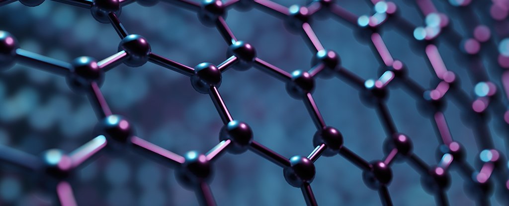
That’s right. This two-dimensional material, consisting of an atomic layer of carbon atoms in a hexagonal lattice, is graphene. Its extraordinary strength and properties have earned it the title “The Wonder Material of the 21st Century.” In the following paragraphs, we’ll go on a journey to explore this marvelous material, from its discovery in 2004 to its remarkable characteristics that have captivated researchers worldwide to its potential applications that could change the world as we know it.
From Scotch Tape to Nobel Prize
In 2004, at the University of Manchester in England, physicists Andre Geim and Konstantin Novoselov isolated a layer of graphene from bulk graphite for the first time, pioneering millions of research studies on two-dimensional materials in the following decades. If you think such a groundbreaking discovery required fancy multi-million-dollar equipment, you’d be wrong. They isolated graphene with a five-dollar piece of equipment that can be found in your office: Scotch Tape.

Geim and Novoselov utilized the tape’s adhesive property to peel thin layers from a block of graphite. Through meticulous repetition, they successfully extracted a single layer of carbon atoms arranged in a hexagonal lattice. This straightforward method, known as mechanical exfoliation, was not initially intended for accurate scientific experiments. However, it sparked a wave of curiosity across the research community, as many realized they could replicate this simple experiment at home. And they were right. A few years later, Geim and Novoselov were awarded the prestigious Nobel Prize in Physics for their groundbreaking discovery, which opened the doors to a realm of limitless possibilities once considered science fiction.
You may wonder why extracting an everyday material into two-dimensional form using office equipment caused so much excitement in the physics community. The answer to that, like many other things, is quantum physics.

Conductivity & Quantum Confinement
Graphene’s conductivity, or the ability to conduct electricity is one of its most transformative features, setting it apart from common conductors such as copper or silicon. This exceptional ability derives from the interplay of quantum physics within its two-dimensional structure, a phenomenon known as quantum confinement. In bulk materials, electrons can move in all three directions, encountering various forms of resistance such as particle scattering and vibration, which reduce conductive efficiency. In graphene, however, electrons are confined to a single atomic layer, allowing them to exhibit unique behaviors not found in traditional materials.
One of these behaviors is the movement of electrons through a material as if they were massless. In graphene, the energy-momentum relationship of electrons is linear, unlike the quadratic relationship found in three-dimensional materials.. This linear relationship causes electrons to behave like Dirac Fermions, moving masslessly at breakneck speeds. This speed, paired with the impurity prevention created by quantum confinement at the two-dimensional level, allows graphene to have a conductivity that surpasses that of all conductors on the market.

Furthermore, graphene is structured so that its conduction bands touch its valence bands, resulting in a zero band gap. Bands, or energy bands, are essentially a range of electron energy levels forming when two particles’ electrons interact quantum mechanically (more details in a later article). If that sounds confusing, don’t worry; all you need to know for this article is that energy bands can be seen as “energy layers”; the conductive band is the higher layer with more energy, while the valence band is the lower layer with less energy. This energy difference, known as a band gap, can form an “invisible barrier” in conductors that creates resistance. However, as mentioned before, graphene doesn’t have this band gap due to its unique structure, which eliminates the resistance that would’ve been present in other conductors, making it the superior choice.

Unparalleled Strength
As mentioned at the beginning of this article, the one-atom thin graphene is the most robust material on earth. To understand why, you first need to understand two types of interactions. The first is known as the van der Waals force, which is the force that connects the countless layers of graphene in graphite. This weak intermolecular force can be broken easily, which is why you can easily exfoliate graphite into a two-dimensional form using tape. However, if you only have one layer of graphene instead of many stacked on each other, these weak van der Waals forces would disappear since there is nothing else for it to connect to.
The second interaction is known as the covalent bond, which connects the carbon atoms in graphene’s hexagonal lattice. The carbon-carbon covalent bond is one of the strongest in nature, with a bond energy of 348 kJ/mol. These robust bonds give graphene an extremely high tensile strength of around 130 GPa and a Young’s Modulus of approximately 1 TPa, surpassing most known materials on earth. Additionally, thanks to graphene’s honeycomb structure, each carbon atom covalently bonds with three other carbon atoms, making the already strong bond even more indestructible.
Promising Applications
Science is of no use if theoretical knowledge cannot be implemented to benefit society; and graphene is no exception. Luckily for us, graphene has many promising applications in fields such as technology and medicine.
Firstly, graphene brings great excitement to the semiconductor industry. Its high carrier mobility, or the speed at which electrons move through the material, allows for a faster, smoother, and more efficient electron flow. Its extremely thin size also enables its implementation at the microscopic scale. This provides flexibility when implementing these semiconductors in technologies and creating more space for semiconductors or other hardware, further enhancing the system’s overall efficiency. Graphene can also address the overheating problem in semiconductors, as its structure has a significantly higher thermal conductivity than other materials, allowing it to dissipate heat generated by electron flow more efficiently.
Graphene is also a promising material for superconductivity, where materials can conduct electricity without resistance, which is a massive deal in physics. In short, superconductivity is achieved in extremely low temperatures through a series of molecular interactions alongside two-dimensional materials’ unique properties (more detail in a future article).
Lastly, like most technologies, scientists are constantly seeking applications of graphene in the health industry since everyone wants to achieve immortality, right? Graphene’s remarkable strength creates durable, flexible scaffolds that can withstand physiological pressure for improved tissue engineering and cell regeneration, a crucial aspect of the health sciences that revives dead cells and organs. On top of that, graphene’s incredible conductivity, the popular option, can be used to activate nerves to enhance the nervous system’s functionality and communication by allowing the flow of faster and more efficient electrical signals.
Ernest Rutherford’s 1908 Nobel Prize in Chemistry wasn’t given for the nuclear power station — he wouldn’t have survived that long — it was given for showing how interesting atomic physics could be. — Andre Geim
References
[1]: Staff, ScienceAlert. “What Is Graphene?” ScienceAlert, www.sciencealert.com/graphene.
[2]: “Graphite vs Graphene.” CTS NEW ZEALAND – Discover the Finest in Fishing, ctsfishing.com/spotlight-on-materials-the-lowdown-on-graphene/graphite-graphene/.
[3]: “The “Accidental” Nobel Laureates: 10 Years On.” Graphene, 6 Dec. 2020, www.google.com/url?q=www.mub.eps.manchester.ac.uk/graphene/2020/12/the-accidental-nobel-laureates-10-years-on/&sa=D&source=docs&ust=1721371184782196&usg=AOvVaw2hzHtbE8FET7IDOYWMV2XA.
[4]: “If the Band-Gap between Valence Band and Conduction Band in a Material Is 5.0 EV Then the Material Is A\/An-A). SemiconductorB). Good ConductorC). SuperconductorD). Insulator.” Www.vedantu.com, www.vedantu.com/question-answer/if-the-bandgap-between-valence-band-and-class-12-physics-cbse-5f502b1bbb9e930be19430b5.
[5]: Walkup, Daniel, and Nikolai B. Zhitenev. “Relativistic Quantum Phenomena in Graphene Quantum Dots.” Nature Nanotechnology, vol. 18, no. 3, 1 Mar. 2023, pp. 219–220, www.nature.com/articles/s41565-023-01317-2, https://doi.org/10.1038/s41565-023-01317-2.


Leave a Reply